Embedded systems and connected devices (IoT) are now ubiquitous. They can be found in smart home appliances, industrial sensors, medical devices, automotive systems and connected urban infrastructure. Behind these devices lie microcontrollers and electronic components whose operation must be rigorously tested, monitored and diagnosed throughout their development cycle.
For engineers and developers, it is essential to be able to analyse the internal behaviour of the hardware, verify firmware execution, or identify the source of a malfunction. This is precisely the role of hardware debugging interfaces, which allow direct interaction with a device’s electronics during the design and validation phases.
However, these mechanisms, designed to facilitate development, can become problematic when they remain accessible on a final product. In the context of connected device security, an exposed debug port can constitute a significant attack surface, particularly for an attacker with physical access to the hardware.
For this reason, these interfaces are now a major focus in IoT penetration testing and embedded system security analysis.
Debug ports are hardware interfaces used in electronics and the IoT to facilitate the development, configuration and diagnosis of embedded systems.
They allow developers to interact directly with a microcontroller or integrated circuit in order to observe its internal operation, analyse firmware execution or modify the system’s state during testing.
Depending on their implementation, these hardware debugging interfaces can offer a wide range of diagnostic or control capabilities over the system:
These features, which are essential during development, also make debug ports particularly sensitive elements in the security of connected devices. When they remain accessible on a device in production, they can offer an attacker a very high level of control over the targeted system.
To understand the risks associated with these interfaces, it is necessary to examine the main types of debug ports found in IoT environments and consumer embedded systems.
JTAG (Joint Test Action Group) is a hardware testing and debugging standard defined in the 1980s and now widely used in embedded systems and modern microcontrollers.
Originally designed to perform continuity tests on printed circuit boards, it has gradually evolved into a comprehensive debugging interface that allows direct interaction with a processor or microcontroller.
Common architectures (ARM, x86, MIPS, PowerPC) thus offer tools for tracing, setting breakpoints, accessing registers and performing memory dumps. This makes JTAG a comprehensive and very powerful tool to support the development and debugging of a printed circuit board.
From a technical perspective, JTAG is a synchronous serial bus that can have 2, 4 or 5 pins:
A standard JTAG configuration looks like this:
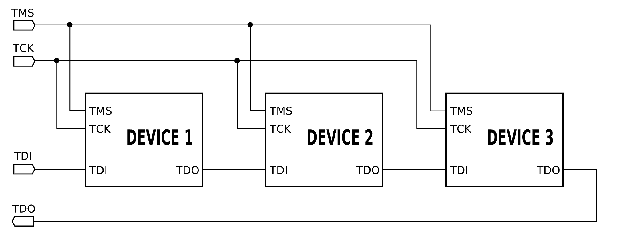
This configuration is generally used in a daisy-chain setup. As the JTAG bus is a serial bus, several components can be connected in series, with the TMS signal used to select the target component.
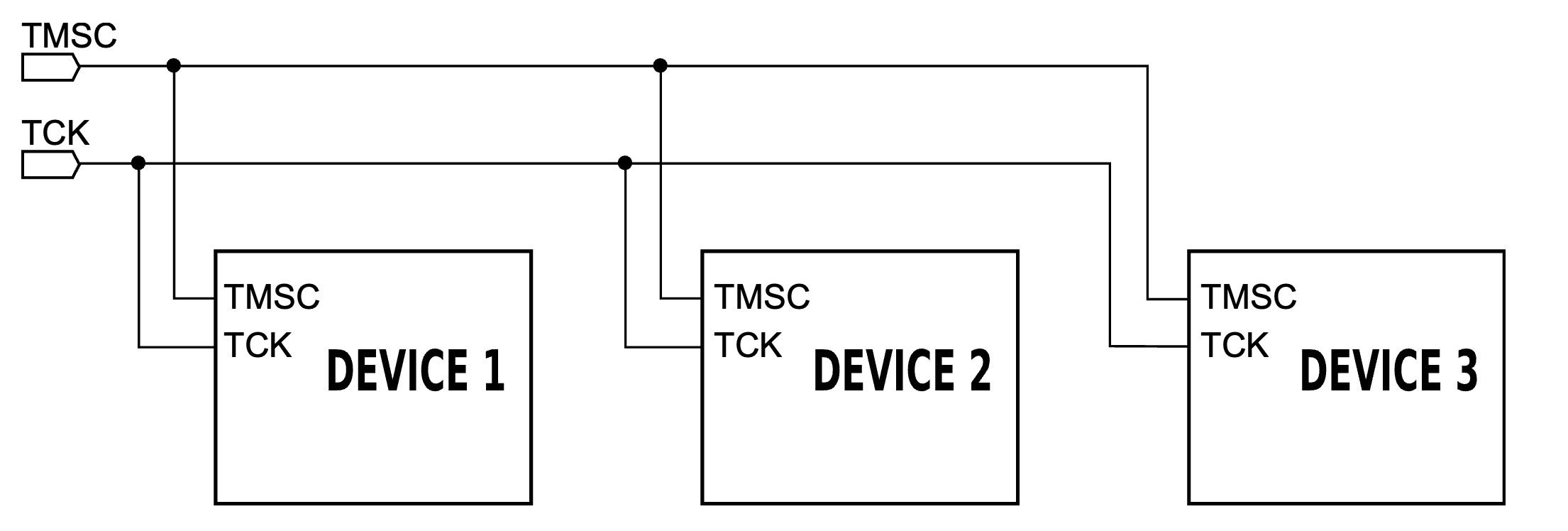
cJTAG (compact JTAG) is a variant of the JTAG protocol designed to reduce the number of pins required.
Unlike standard JTAG, it uses only two lines:
As there is only a single communication channel (without TMS), when multiple components are present, all components must be powered on and parse the instructions sent via the TMSC channel; this is the only way to determine which specific component the instructions are addressed to.
This simplification reduces the physical footprint on integrated circuits, which is particularly useful in compact embedded systems.
The UART (Universal Asynchronous Receiver-Transmitter) is an asynchronous serial communication interface widely used in embedded systems and connected devices.
Unlike JTAG or SWD, the UART is not a dedicated debug interface but simply a communication channel between two components. It has been in use since the 1980s to enable communication between a computer and a peripheral device.
As it is asynchronous, there is no pin to synchronise the communication frequency. The system requires only two pins:
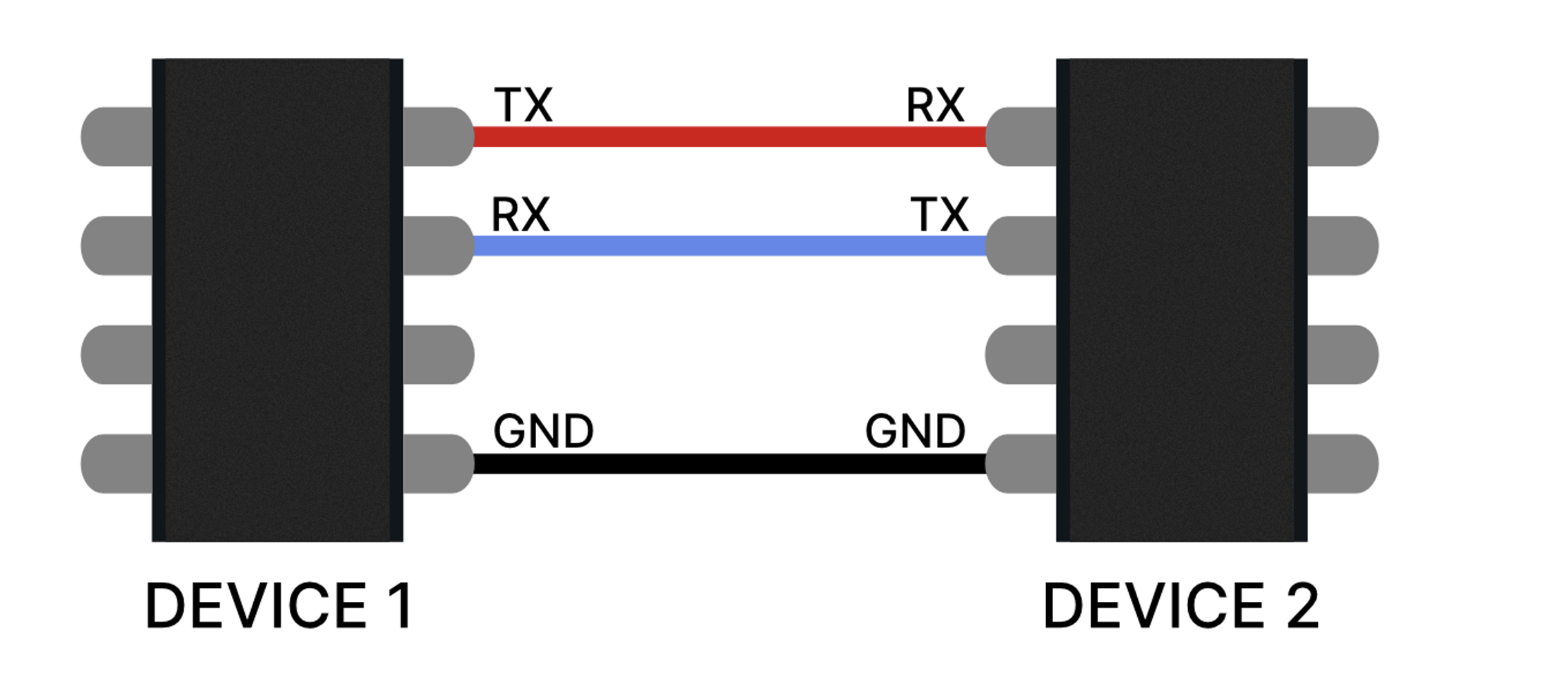
Each pin is connected to its counterpart on the remote device.
As there is no dedicated pin for frequency synchronisation, this must be set up manually to ensure that the two components can communicate correctly. Synchronisation between the two systems is therefore established via a baud rate, which is often set to 115,200 baud in embedded systems.
The UART is a simple communication system. It has no predefined functions such as those found, for example, in JTAG with EXTEST. Any functionality will therefore be defined either by the manufacturer of the target component or by the software running on it. There are, of course, numerous implementation standards—too many to list—and this is without taking into account any additional layers of functionality that may be added later.
In many IoT devices, a UART port exposed on the circuit board provides access to a serial console. This can display firmware logs, allow interaction with a bootloader or, in some cases, provide direct access to a system shell. It can be difficult for a malicious actor (without access to the documentation) to know what privileges or opportunities an active UART port might afford them.
SWD (Serial Wire Debug) is a debug interface developed by ARM for Cortex-M microcontrollers.
It uses two main lines:
It incorporates the main debugging capabilities of JTAG whilst reducing the number of pins required, making it particularly well-suited to modern microcontrollers used in connected devices. However, it does not allow continuity testing. It is also limited to ARM architectures; to my knowledge, no other manufacturers have decided to implement this protocol.
This interface enables numerous ARM debugging operations, such as accessing processor registers, inspecting memory or analysing firmware whilst it is running.
JTAG, UART and SWD are the main types of debug ports, but there are other standards developed by various companies or consortia. Technically, any manufacturer can implement its own debugging tools, which can lead to a proliferation of such tools, each with documentation that is more or less comprehensive and more or less publicly available.
Among the relatively widespread standards:
Debug ports provide a set of extremely powerful tools for interacting with an embedded system. When left accessible on a device in production, they can give an attacker with physical access a significant advantage.
During an IoT penetration test, these interfaces are often among the first elements to be analysed. An active port can enable:
A fully functional JTAG port, for example, can lead to the complete compromise of the targeted component, which can then be exploited to compromise other elements of the system or the ecosystem to which it belongs.
To draw a parallel with the world of the web, a debug port should be regarded as the equivalent of a development mode enabled on an application or a framework (such as the Symfony profiler). It is an extremely useful tool during development but must be disabled or protected before going live.
It is therefore essential to implement security processes during deployment to ensure that debug interfaces do not remain accessible in commercial products. Poor management of these ports can lead to the leakage of sensitive data, the compromise of firmware, or even the use of the component as an entry point for wider attacks.
Debug ports are essential tools for the development and analysis of embedded systems. They enable engineers to observe the internal workings of a microcontroller, access the firmware and diagnose hardware or software issues.
However, when they remain accessible in a final product, they can provide an attacker with privileged access to the hardware and firmware. In the field of IoT security, disabling, restricting or protecting them is therefore an essential step in limiting the risks associated with physical access to the device.
Author: Renaud CAYOL – Pentester @Vaadata


